

Shara Circuits Pvt.Ltd
PCB FABRICATION
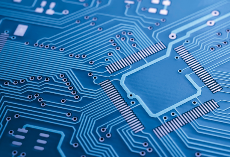
Shara Circuits Pvt. Ltd. is a renowned manufacturer and supplier of high-quality PCB (Printed Circuit Board) fabrication services. With years of industry experience and cutting-edge technology, we specialize in delivering precision-engineered PCBs that meet the diverse needs of various sectors, including electronics, automotive, telecommunications, medical devices, and more.
Our PCB fabrication services are known for their reliability, efficiency, and exceptional performance. We offer a wide range of PCB types, from single-sided to multi-layered designs, ensuring we can accommodate projects of any complexity. Our commitment to quality, precision, and timely delivery sets us apart as a leading player in the PCB fabrication industry.
At Shara Circuits, we use advanced manufacturing techniques and the latest machinery to ensure every PCB is fabricated to the highest standards. Whether you’re looking for a small batch or large-scale production, our team works closely with you to deliver customized solutions that exceed your expectations.
Manufacturing Capacity
At Shara Circuits, we pride ourselves on producing PCBs using traditional materials like FR4 PCB and advanced FR4-High TG-170 PCBs. Our offerings range from 4-layer to 32-layer Multilayer PCBs, Impedance Control PCBs, Anylayer HDI PCBs, and Micro-via Blind/Buried hole PCBs. We also specialize in PCBs with transparent ink solder masks, carbon ink, and the unique blue peelable mask.
For any inquiries or detailed information, connect with us directly at info@sharacircuits.com.
Our commitment to excellence has led us to invest in cutting-edge machinery and develop a vertically integrated infrastructure. This synergy of state-of-the-art technology and expert personnel drives our ambition to be a top-tier, all-inclusive PCB & PCBA service provider for both local and international clientele.
Understanding our offerings:
Single-sided PCBs: Typically made from single-sided copper-clad laminate, these boards have circuits on one side and plug-in components on the other.
Double-sided PCBs: These are crafted from double-sided copper-clad laminates and have two circuit patterns – the Component Side and the Solder Side. The walls of the vias in these boards are copper-plated, facilitating conduction between the top and bottom layers.
Multi-layer PCBs: Building on the foundation of double-sided boards, multi-layer PCBs incorporate an internal power layer and ground layer. They consist of at least three or more circuit layers. Vias ensure conductivity across each substrate layer, and these layers are seamlessly fused through a lamination process, with insulating material positioned between each layer. The design and routing of these boards aim to optimize internal electrical layer pathways, promoting more efficient circuit board routing and paving the way for products with large capacities in compact sizes.
With the evolution of electronic technology and the proliferation of integrated circuits, our multilayer PCBs are swiftly advancing towards high-precision and high-density digital integration. This progression is evident in the increasing fine line widths, reduced line spacing, micro aperture penetrations, and the adoption of HDI technology to cater to the ever-evolving market needs.